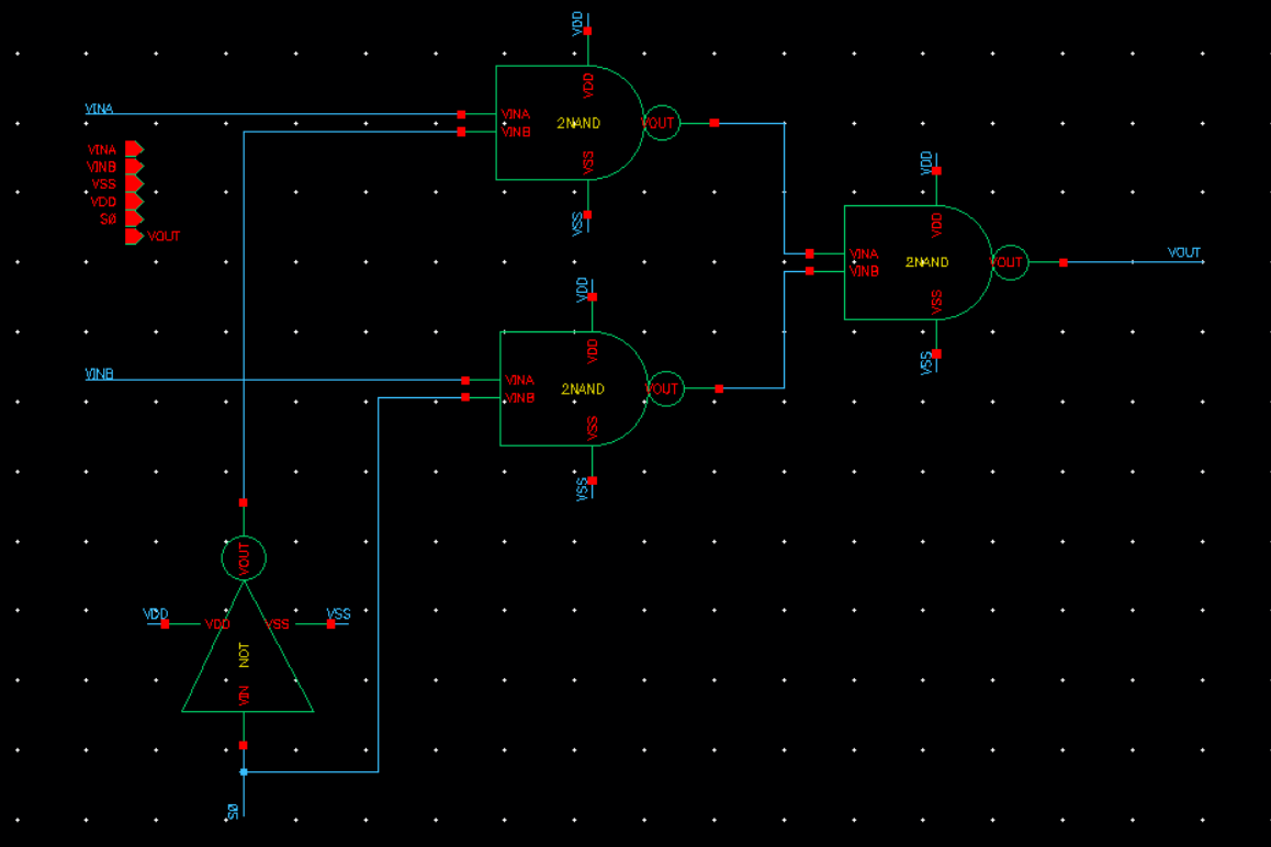
Schematic
Schematic 구성
- 2NAND 3개
- NOT 1개
Symbol

Simualtion 측정 과정

VNIB Propertise / S0 Propertise 설정


파형을 확인할 때는 최소한 5~10주기는 확인해야하기 때문에 VINB Period와 Pulse width를 S0 Propertise에서는 10배로 설정한다.
Choosing Analyses 설정

Simualtion

Layout

- Layout size : 가로 : 4.63 µm
세로 5.87 µm
4.63*5.87 = 27.1781 µm^2 - Transistor 14 개 사용
'Custom IC one-chip 설계 > DIGITAL LOGIC GATE' 카테고리의 다른 글
| [Digital Logic Gate]_4x1Multiplexer_Switch (0) | 2025.04.28 |
|---|---|
| [Digital Logic Gate]_4x1Multiplexer_LOGIC (0) | 2025.04.28 |
| [Digital Logic Gate]_4NOR (0) | 2025.04.24 |
| [Digital Logic Gate]_4NAND (0) | 2025.04.24 |
| [Digital Logic Gate]_3NOR (0) | 2025.04.24 |