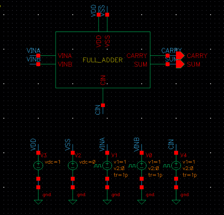
Schematic

Symbol

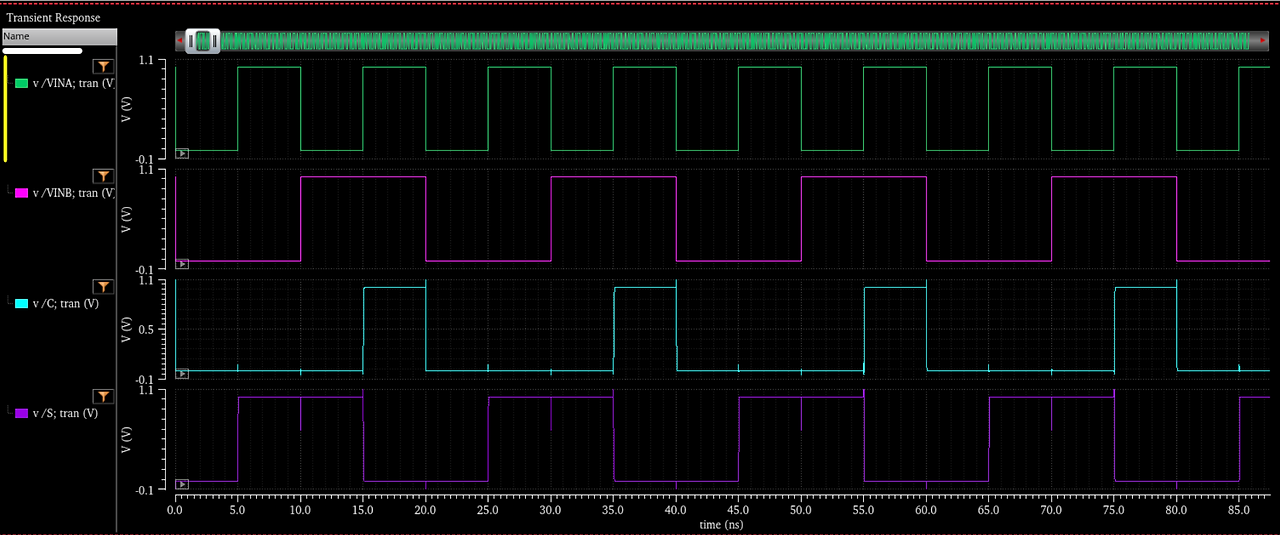
Simualtion
Propertise 설정


Layout

- Layout size : 가로 11.11 µm
세로 7.315 µm
11.11 * 7.315 = 81.269 µm^2
'Custom IC one-chip 설계 > DIGITAL LOGIC GATE' 카테고리의 다른 글
| [Digital Logic Gate]_4BIT_ADDER_SUBTRACTOR (0) | 2025.06.04 |
|---|---|
| [Digital Logic Gate]_4BIT_ADDER (0) | 2025.06.04 |
| [Digital Logic Gate]_HALF_ADDER (0) | 2025.06.04 |
| [Digital Logic Gate]_XOR (0) | 2025.05.11 |
| [Digital Logic Gate]_16x1Multiplexer_Switch (0) | 2025.05.11 |