목적
- DHT11 온습도 센서를 MicroBlaze RISC-V 기반 SoC 시스템에서 AXI-Lite 인터페이스를 통해 제어하고, 습도 및 온도 데이터를 읽어 UART로 출력
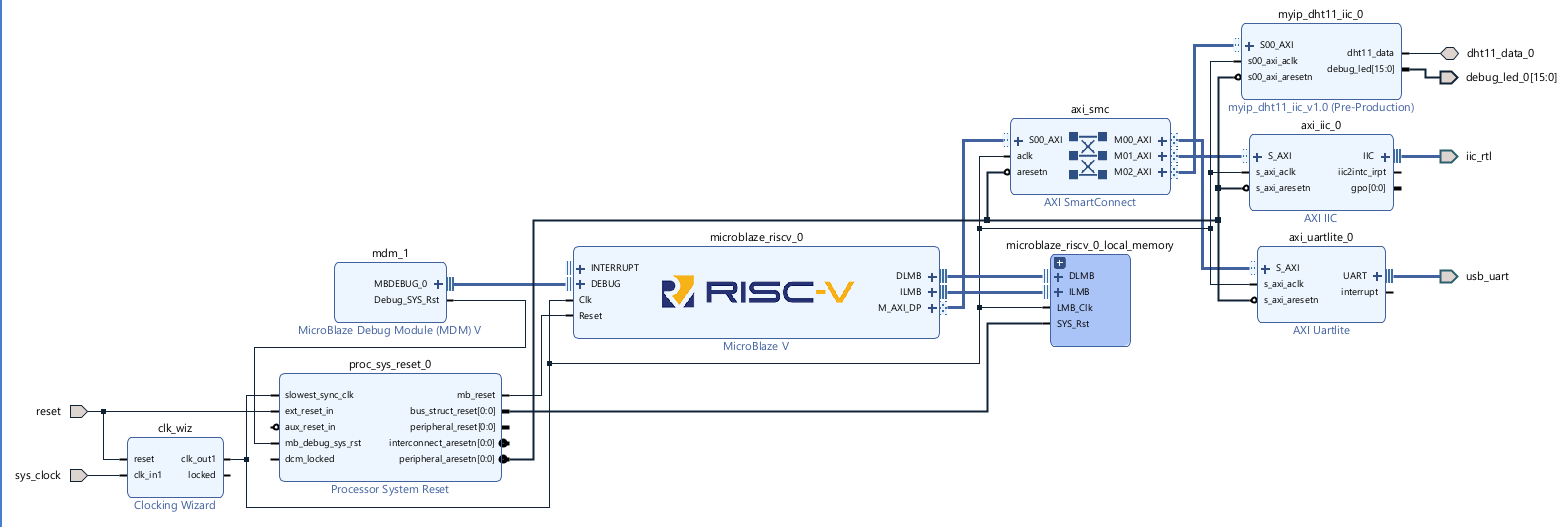
Diagram
사용 코드_myip_dht11_iic
`timescale 1 ns / 1 ps

	module myip_dht11_iic #
	(
		// Users to add parameters here

		// User parameters ends
		// Do not modify the parameters beyond this line


		// Parameters of Axi Slave Bus Interface S00_AXI
		parameter integer C_S00_AXI_DATA_WIDTH	= 32,
		parameter integer C_S00_AXI_ADDR_WIDTH	= 5
	)
	(
		// Users to add ports here
        inout dht11_data,
		output [15:0] debug_led,
		// User ports ends
		// Do not modify the ports beyond this line


		// Ports of Axi Slave Bus Interface S00_AXI
		input wire  s00_axi_aclk,
		input wire  s00_axi_aresetn,
		input wire [C_S00_AXI_ADDR_WIDTH-1 : 0] s00_axi_awaddr,
		input wire [2 : 0] s00_axi_awprot,
		input wire  s00_axi_awvalid,
		output wire  s00_axi_awready,
		input wire [C_S00_AXI_DATA_WIDTH-1 : 0] s00_axi_wdata,
		input wire [(C_S00_AXI_DATA_WIDTH/8)-1 : 0] s00_axi_wstrb,
		input wire  s00_axi_wvalid,
		output wire  s00_axi_wready,
		output wire [1 : 0] s00_axi_bresp,
		output wire  s00_axi_bvalid,
		input wire  s00_axi_bready,
		input wire [C_S00_AXI_ADDR_WIDTH-1 : 0] s00_axi_araddr,
		input wire [2 : 0] s00_axi_arprot,
		input wire  s00_axi_arvalid,
		output wire  s00_axi_arready,
		output wire [C_S00_AXI_DATA_WIDTH-1 : 0] s00_axi_rdata,
		output wire [1 : 0] s00_axi_rresp,
		output wire  s00_axi_rvalid,
		input wire  s00_axi_rready
	);
// Instantiation of Axi Bus Interface S00_AXI
	myip_dht11_iic_slave_lite_v1_0_S00_AXI # (
		.C_S_AXI_DATA_WIDTH(C_S00_AXI_DATA_WIDTH),
		.C_S_AXI_ADDR_WIDTH(C_S00_AXI_ADDR_WIDTH)
	) myip_dht11_iic_slave_lite_v1_0_S00_AXI_inst (
	   .dht11_data(dht11_data),
		.debug_led(debug_led),

		.S_AXI_ACLK(s00_axi_aclk),
		.S_AXI_ARESETN(s00_axi_aresetn),
		.S_AXI_AWADDR(s00_axi_awaddr),
		.S_AXI_AWPROT(s00_axi_awprot),
		.S_AXI_AWVALID(s00_axi_awvalid),
		.S_AXI_AWREADY(s00_axi_awready),
		.S_AXI_WDATA(s00_axi_wdata),
		.S_AXI_WSTRB(s00_axi_wstrb),
		.S_AXI_WVALID(s00_axi_wvalid),
		.S_AXI_WREADY(s00_axi_wready),
		.S_AXI_BRESP(s00_axi_bresp),
		.S_AXI_BVALID(s00_axi_bvalid),
		.S_AXI_BREADY(s00_axi_bready),
		.S_AXI_ARADDR(s00_axi_araddr),
		.S_AXI_ARPROT(s00_axi_arprot),
		.S_AXI_ARVALID(s00_axi_arvalid),
		.S_AXI_ARREADY(s00_axi_arready),
		.S_AXI_RDATA(s00_axi_rdata),
		.S_AXI_RRESP(s00_axi_rresp),
		.S_AXI_RVALID(s00_axi_rvalid),
		.S_AXI_RREADY(s00_axi_rready)
	);

	// Add user logic here

	// User logic ends

	endmodule
사용 코드 _myip_dht11_iic_slave_lite_v1_0_S00_AXI
`timescale 1 ns / 1 ps

	module myip_dht11_iic_slave_lite_v1_0_S00_AXI #
	(
		// Users to add parameters here

		// User parameters ends
		// Do not modify the parameters beyond this line

		// Width of S_AXI data bus
		parameter integer C_S_AXI_DATA_WIDTH	= 32,
		// Width of S_AXI address bus
		parameter integer C_S_AXI_ADDR_WIDTH	= 5
	)
	(
		// Users to add ports here
        inout dht11_data,
		output [15:0] debug_led,
		// User ports ends
		// Do not modify the ports beyond this line

		// Global Clock Signal
		input wire  S_AXI_ACLK,
		// Global Reset Signal. This Signal is Active LOW
		input wire  S_AXI_ARESETN,
		// Write address (issued by master, acceped by Slave)
		input wire [C_S_AXI_ADDR_WIDTH-1 : 0] S_AXI_AWADDR,
		// Write channel Protection type. This signal indicates the
    		// privilege and security level of the transaction, and whether
    		// the transaction is a data access or an instruction access.
		input wire [2 : 0] S_AXI_AWPROT,
		// Write address valid. This signal indicates that the master signaling
    		// valid write address and control information.
		input wire  S_AXI_AWVALID,
		// Write address ready. This signal indicates that the slave is ready
    		// to accept an address and associated control signals.
		output wire  S_AXI_AWREADY,
		// Write data (issued by master, acceped by Slave)
		input wire [C_S_AXI_DATA_WIDTH-1 : 0] S_AXI_WDATA,
		// Write strobes. This signal indicates which byte lanes hold
    		// valid data. There is one write strobe bit for each eight
    		// bits of the write data bus.
		input wire [(C_S_AXI_DATA_WIDTH/8)-1 : 0] S_AXI_WSTRB,
		// Write valid. This signal indicates that valid write
    		// data and strobes are available.
		input wire  S_AXI_WVALID,
		// Write ready. This signal indicates that the slave
    		// can accept the write data.
		output wire  S_AXI_WREADY,
		// Write response. This signal indicates the status
    		// of the write transaction.
		output wire [1 : 0] S_AXI_BRESP,
		// Write response valid. This signal indicates that the channel
    		// is signaling a valid write response.
		output wire  S_AXI_BVALID,
		// Response ready. This signal indicates that the master
    		// can accept a write response.
		input wire  S_AXI_BREADY,
		// Read address (issued by master, acceped by Slave)
		input wire [C_S_AXI_ADDR_WIDTH-1 : 0] S_AXI_ARADDR,
		// Protection type. This signal indicates the privilege
    		// and security level of the transaction, and whether the
    		// transaction is a data access or an instruction access.
		input wire [2 : 0] S_AXI_ARPROT,
		// Read address valid. This signal indicates that the channel
    		// is signaling valid read address and control information.
		input wire  S_AXI_ARVALID,
		// Read address ready. This signal indicates that the slave is
    		// ready to accept an address and associated control signals.
		output wire  S_AXI_ARREADY,
		// Read data (issued by slave)
		output wire [C_S_AXI_DATA_WIDTH-1 : 0] S_AXI_RDATA,
		// Read response. This signal indicates the status of the
    		// read transfer.
		output wire [1 : 0] S_AXI_RRESP,
		// Read valid. This signal indicates that the channel is
    		// signaling the required read data.
		output wire  S_AXI_RVALID,
		// Read ready. This signal indicates that the master can
    		// accept the read data and response information.
		input wire  S_AXI_RREADY
	);

    wire [7:0] humidity, temperature;

	// AXI4LITE signals
	reg [C_S_AXI_ADDR_WIDTH-1 : 0] 	axi_awaddr;
	reg  	axi_awready;
	reg  	axi_wready;
	reg [1 : 0] 	axi_bresp;
	reg  	axi_bvalid;
	reg [C_S_AXI_ADDR_WIDTH-1 : 0] 	axi_araddr;
	reg  	axi_arready;
	reg [1 : 0] 	axi_rresp;
	reg  	axi_rvalid;

	// Example-specific design signals
	// local parameter for addressing 32 bit / 64 bit C_S_AXI_DATA_WIDTH
	// ADDR_LSB is used for addressing 32/64 bit registers/memories
	// ADDR_LSB = 2 for 32 bits (n downto 2)
	// ADDR_LSB = 3 for 64 bits (n downto 3)
	localparam integer ADDR_LSB = (C_S_AXI_DATA_WIDTH/32) + 1;
	localparam integer OPT_MEM_ADDR_BITS = 2;
	//----------------------------------------------
	//-- Signals for user logic register space example
	//------------------------------------------------
	//-- Number of Slave Registers 8
	reg [C_S_AXI_DATA_WIDTH-1:0]	slv_reg0;
	reg [C_S_AXI_DATA_WIDTH-1:0]	slv_reg1;
	reg [C_S_AXI_DATA_WIDTH-1:0]	slv_reg2;
	reg [C_S_AXI_DATA_WIDTH-1:0]	slv_reg3;
	reg [C_S_AXI_DATA_WIDTH-1:0]	slv_reg4;
	reg [C_S_AXI_DATA_WIDTH-1:0]	slv_reg5;
	reg [C_S_AXI_DATA_WIDTH-1:0]	slv_reg6;
	reg [C_S_AXI_DATA_WIDTH-1:0]	slv_reg7;
	integer	 byte_index;

	// I/O Connections assignments

	assign S_AXI_AWREADY	= axi_awready;
	assign S_AXI_WREADY	= axi_wready;
	assign S_AXI_BRESP	= axi_bresp;
	assign S_AXI_BVALID	= axi_bvalid;
	assign S_AXI_ARREADY	= axi_arready;
	assign S_AXI_RRESP	= axi_rresp;
	assign S_AXI_RVALID	= axi_rvalid;
	 //state machine varibles
	 reg [1:0] state_write;
	 reg [1:0] state_read;
	 //State machine local parameters
	 localparam Idle = 2'b00,Raddr = 2'b10,Rdata = 2'b11 ,Waddr = 2'b10,Wdata = 2'b11;
	// Implement Write state machine
	// Outstanding write transactions are not supported by the slave i.e., master should assert bready to receive response on or before it starts sending the new transaction
	always @(posedge S_AXI_ACLK)
	  begin
	     if (S_AXI_ARESETN == 1'b0)
	       begin
	         axi_awready <= 0;
	         axi_wready <= 0;
	         axi_bvalid <= 0;
	         axi_bresp <= 0;
	         axi_awaddr <= 0;
	         state_write <= Idle;
	       end
	     else
	       begin
	         case(state_write)
	           Idle:
	             begin
	               if(S_AXI_ARESETN == 1'b1)
	                 begin
	                   axi_awready <= 1'b1;
	                   axi_wready <= 1'b1;
	                   state_write <= Waddr;
	                 end
	               else state_write <= state_write;
	             end
	           Waddr:        //At this state, slave is ready to receive address along with corresponding control signals and first data packet. Response valid is also handled at this state
	             begin
	               if (S_AXI_AWVALID && S_AXI_AWREADY)
	                  begin
	                    axi_awaddr <= S_AXI_AWADDR;
	                    if(S_AXI_WVALID)
	                      begin
	                        axi_awready <= 1'b1;
	                        state_write <= Waddr;
	                        axi_bvalid <= 1'b1;
	                      end
	                    else
	                      begin
	                        axi_awready <= 1'b0;
	                        state_write <= Wdata;
	                        if (S_AXI_BREADY && axi_bvalid) axi_bvalid <= 1'b0;
	                      end
	                  end
	               else
	                  begin
	                    state_write <= state_write;
	                    if (S_AXI_BREADY && axi_bvalid) axi_bvalid <= 1'b0;
	                   end
	             end
	          Wdata:        //At this state, slave is ready to receive the data packets until the number of transfers is equal to burst length
	             begin
	               if (S_AXI_WVALID)
	                 begin
	                   state_write <= Waddr;
	                   axi_bvalid <= 1'b1;
	                   axi_awready <= 1'b1;
	                 end
	                else
	                 begin
	                   state_write <= state_write;
	                   if (S_AXI_BREADY && axi_bvalid) axi_bvalid <= 1'b0;
	                 end
	             end
	          endcase
	        end
	      end

	// Implement memory mapped register select and write logic generation
	// The write data is accepted and written to memory mapped registers when
	// axi_awready, S_AXI_WVALID, axi_wready and S_AXI_WVALID are asserted. Write strobes are used to
	// select byte enables of slave registers while writing.
	// These registers are cleared when reset (active low) is applied.
	// Slave register write enable is asserted when valid address and data are available
	// and the slave is ready to accept the write address and write data.


	always @( posedge S_AXI_ACLK )
	begin
	  if ( S_AXI_ARESETN == 1'b0 )
	    begin
	      slv_reg0 <= 0;
	      slv_reg1 <= 0;
	      slv_reg2 <= 0;
	      slv_reg3 <= 0;
	      slv_reg4 <= 0;
	      slv_reg5 <= 0;
	      slv_reg6 <= 0;
	      slv_reg7 <= 0;
	    end
	  else begin
	    if (S_AXI_WVALID)
	      begin
	        case ( (S_AXI_AWVALID) ? S_AXI_AWADDR[ADDR_LSB+OPT_MEM_ADDR_BITS:ADDR_LSB] : axi_awaddr[ADDR_LSB+OPT_MEM_ADDR_BITS:ADDR_LSB] )
	          3'h0:
	            for ( byte_index = 0; byte_index <= (C_S_AXI_DATA_WIDTH/8)-1; byte_index = byte_index+1 )
	              if ( S_AXI_WSTRB[byte_index] == 1 ) begin
	                // Respective byte enables are asserted as per write strobes
	                // Slave register 0
	                slv_reg0[(byte_index*8) +: 8] <= S_AXI_WDATA[(byte_index*8) +: 8];
	              end
	          3'h1:
	            for ( byte_index = 0; byte_index <= (C_S_AXI_DATA_WIDTH/8)-1; byte_index = byte_index+1 )
	              if ( S_AXI_WSTRB[byte_index] == 1 ) begin
	                // Respective byte enables are asserted as per write strobes
	                // Slave register 1
	                slv_reg1[(byte_index*8) +: 8] <= S_AXI_WDATA[(byte_index*8) +: 8];
	              end
	          3'h2:
	            for ( byte_index = 0; byte_index <= (C_S_AXI_DATA_WIDTH/8)-1; byte_index = byte_index+1 )
	              if ( S_AXI_WSTRB[byte_index] == 1 ) begin
	                // Respective byte enables are asserted as per write strobes
	                // Slave register 2
	                slv_reg2[(byte_index*8) +: 8] <= S_AXI_WDATA[(byte_index*8) +: 8];
	              end
	          3'h3:
	            for ( byte_index = 0; byte_index <= (C_S_AXI_DATA_WIDTH/8)-1; byte_index = byte_index+1 )
	              if ( S_AXI_WSTRB[byte_index] == 1 ) begin
	                // Respective byte enables are asserted as per write strobes
	                // Slave register 3
	                slv_reg3[(byte_index*8) +: 8] <= S_AXI_WDATA[(byte_index*8) +: 8];
	              end
	          3'h4:
	            for ( byte_index = 0; byte_index <= (C_S_AXI_DATA_WIDTH/8)-1; byte_index = byte_index+1 )
	              if ( S_AXI_WSTRB[byte_index] == 1 ) begin
	                // Respective byte enables are asserted as per write strobes
	                // Slave register 4
	                slv_reg4[(byte_index*8) +: 8] <= S_AXI_WDATA[(byte_index*8) +: 8];
	              end
	          3'h5:
	            for ( byte_index = 0; byte_index <= (C_S_AXI_DATA_WIDTH/8)-1; byte_index = byte_index+1 )
	              if ( S_AXI_WSTRB[byte_index] == 1 ) begin
	                // Respective byte enables are asserted as per write strobes
	                // Slave register 5
	                slv_reg5[(byte_index*8) +: 8] <= S_AXI_WDATA[(byte_index*8) +: 8];
	              end
	          3'h6:
	            for ( byte_index = 0; byte_index <= (C_S_AXI_DATA_WIDTH/8)-1; byte_index = byte_index+1 )
	              if ( S_AXI_WSTRB[byte_index] == 1 ) begin
	                // Respective byte enables are asserted as per write strobes
	                // Slave register 6
	                slv_reg6[(byte_index*8) +: 8] <= S_AXI_WDATA[(byte_index*8) +: 8];
	              end
	          3'h7:
	            for ( byte_index = 0; byte_index <= (C_S_AXI_DATA_WIDTH/8)-1; byte_index = byte_index+1 )
	              if ( S_AXI_WSTRB[byte_index] == 1 ) begin
	                // Respective byte enables are asserted as per write strobes
	                // Slave register 7
	                slv_reg7[(byte_index*8) +: 8] <= S_AXI_WDATA[(byte_index*8) +: 8];
	              end
	          default : begin
	                      slv_reg0 <= slv_reg0;
	                      slv_reg1 <= slv_reg1;
	                      slv_reg2 <= slv_reg2;
	                      slv_reg3 <= slv_reg3;
	                      slv_reg4 <= slv_reg4;
	                      slv_reg5 <= slv_reg5;
	                      slv_reg6 <= slv_reg6;
	                      slv_reg7 <= slv_reg7;
	                    end
	        endcase
	      end
	  end
	end

	// Implement read state machine
	  always @(posedge S_AXI_ACLK)
	    begin
	      if (S_AXI_ARESETN == 1'b0)
	        begin
	         //asserting initial values to all 0's during reset
	         axi_arready <= 1'b0;
	         axi_rvalid <= 1'b0;
	         axi_rresp <= 1'b0;
	         state_read <= Idle;
	        end
	      else
	        begin
	          case(state_read)
	            Idle:     //Initial state inidicating reset is done and ready to receive read/write transactions
	              begin
	                if (S_AXI_ARESETN == 1'b1)
	                  begin
	                    state_read <= Raddr;
	                    axi_arready <= 1'b1;
	                  end
	                else state_read <= state_read;
	              end
	            Raddr:        //At this state, slave is ready to receive address along with corresponding control signals
	              begin
	                if (S_AXI_ARVALID && S_AXI_ARREADY)
	                  begin
	                    state_read <= Rdata;
	                    axi_araddr <= S_AXI_ARADDR;
	                    axi_rvalid <= 1'b1;
	                    axi_arready <= 1'b0;
	                  end
	                else state_read <= state_read;
	              end
	            Rdata:        //At this state, slave is ready to send the data packets until the number of transfers is equal to burst length
	              begin
	                if (S_AXI_RVALID && S_AXI_RREADY)
	                  begin
	                    axi_rvalid <= 1'b0;
	                    axi_arready <= 1'b1;
	                    state_read <= Raddr;
	                  end
	                else state_read <= state_read;
	              end
	           endcase
	          end
	        end
	// Implement memory mapped register select and read logic generation
	  assign S_AXI_RDATA = (axi_araddr[ADDR_LSB+OPT_MEM_ADDR_BITS:ADDR_LSB] == 3'h0) ? humidity :
	       (axi_araddr[ADDR_LSB+OPT_MEM_ADDR_BITS:ADDR_LSB] == 3'h1) ? temperature :
	       (axi_araddr[ADDR_LSB+OPT_MEM_ADDR_BITS:ADDR_LSB] == 3'h2) ? slv_reg2 :
	       (axi_araddr[ADDR_LSB+OPT_MEM_ADDR_BITS:ADDR_LSB] == 3'h3) ? slv_reg3 :
	       (axi_araddr[ADDR_LSB+OPT_MEM_ADDR_BITS:ADDR_LSB] == 3'h4) ? slv_reg4 :
	       (axi_araddr[ADDR_LSB+OPT_MEM_ADDR_BITS:ADDR_LSB] == 3'h5) ? slv_reg5 :
	       (axi_araddr[ADDR_LSB+OPT_MEM_ADDR_BITS:ADDR_LSB] == 3'h6) ? slv_reg6 :
	       (axi_araddr[ADDR_LSB+OPT_MEM_ADDR_BITS:ADDR_LSB] == 3'h7) ? 32'h1234 : 0;
	// Add user logic here
    dht11_cntr dht11(      //fsm, asm은 알고리즘대로 그래서 상태가 많아서, fsm유한 상태 머신
        .clk(S_AXI_ACLK),
        .reset_p(~S_AXI_ARESETN),          //input도 reg선언이 안된다. inout도 입력이 있기 때문에 wire만 된다.
        .dht11_data(dht11_data),       //inout 포트는 reg선언이 안된다.
        .humidity(humidity),
        .temperature(temperature),
        .debug_led(debug_led)   );
	// User logic ends

	endmodule
사용 코드_ Vitis
#include <stdio.h>               // 표준 입출력 함수 사용
#include "platform.h"           // 플랫폼 초기화 및 종료 함수 포함
#include "xil_printf.h"         // Xilinx 전용 출력 함수 (xil_printf)
#include "xparameters.h"        // 하드웨어 주소 등 시스템 파라미터 정의
#include "sleep.h"              // sleep 함수 사용을 위한 헤더

// DHT11 IP 코어의 베이스 주소를 정의 (xparameters.h에서 자동 정의된 매크로 사용)
#define dht_addr XPAR_MYIP_DHT11_IIC_0_BASEADDR

int main()
{
    // 플랫폼 초기화 (UART 설정 등 기본 하드웨어 설정)
    init_platform();

    // UART를 통해 간단한 출력 확인
    print("Hello World\n\r");
    print("Successfully ran Hello World application");

    // DHT11 센서 데이터를 읽을 수 있는 메모리 주소 포인터 생성
    // 이 주소는 사용자 정의 IP 코어가 메모리 맵에 매핑된 위치
    volatile unsigned int *dht11_instance = (volatile unsigned int*) dht_addr;

    while(1){
        // DHT11 센서의 습도 값을 읽어 UART로 출력 (레지스터 0번)
        xil_printf("Humidity : %d\n\r", dht11_instance[0]);

        // DHT11 센서의 온도 값을 읽어 UART로 출력 (레지스터 1번)
        xil_printf("Temperature : %d\n\r", dht11_instance[1]);

        // 3초 대기 (센서 업데이트 주기에 맞춰 딜레이)
        sleep(3);
    }

    // 플랫폼 종료 처리 (자원 정리 등)
    cleanup_platform();
    return 0;
}
동작 영상
결과
사용자 정의 IP(myip_dht11_iic_0) 내부에 구현된 FSM(dht11_cntr)이 DHT11 센서에 대해 아래 프로토콜을 자동으로 수행합니다:
- 센서 초기화한다.
- 데이터 요청 신호 전송한다.
- 센서 응답 대기 및 데이터 수신한다.
- 습도 및 온도 값 저장 (humidity, temperature)한다.
- dht11_instance[0]에서 습도 값을 읽는다,
- dht11_instance[1]에서 온도 값을 읽는다.
- 두 값을 UART로 PC에 출력되는 것을 확인 할 수 있다.
'Verilog_RTL 설계 > SoC' 카테고리의 다른 글
| [Project]Smart Mobility platform (4) | 2025.08.27 |
|---|---|
| [Smart Mobility platform] Implemented Code (4) | 2025.08.07 |
| [MicroBlaze] Button_control (1) | 2025.07.28 |
| [MicroBlaze] fnd_control (1) | 2025.07.28 |
| [MicroBlaze] Switch_Led (2) | 2025.07.25 |